IC 7408 is a logic gate chip with four two-input AND gates. Each of the four AND gates are independent. Each gate has one output, two inputs and three pins. The AND gates carry out logic AND operation. Logic gates are available in the form of ICs.
IC 7408 datasheet
According to its datasheet, some of the main specs of the chip are:
- Low power consumption
- TTL outputs
- Recommended operating voltage is 5V
- The maximum current allowed to draw through each gate output is 8mA
- Operating voltage range of 4.75V to 5.25V
- Maximum supply voltage of 7V
- Typical fall time is 18ns
- Typical rise time is 18ns
The following are the key application areas for the chip:
- Electronic devices
- Digital electronic projects
- Digital systems
- Networking
- Memory units
- General-purpose AND logic operation
- Measuring instruments
- Servers
- ALUs
IC 7408 pinout
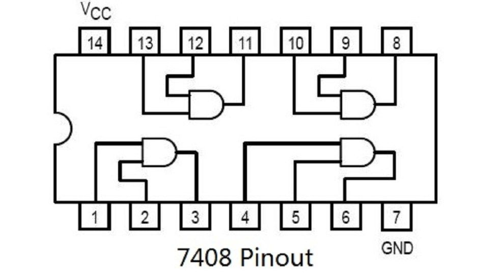
IC 7408 has fourteen pins, including the ground and Vcc pins. Pin 1 is the input of the first AND gate, pin 2 is the second input, and pin 3 is the output of the first AND gate. Pin 4 to 6 are the inputs and outputs of the second AND gate. Pin 7 is the ground pin that provides power to the chip. Pin 14 is the Vcc terminal of the chip, and it is used to provide the chip with a power supply.
Have a look at the IC 7408 pinout diagram above.
IC 7408 Equivalents and Replacement Details
Equivalents of IC 7408 are IC 74LS08, HEF4081, and SN54LS08. Any of the two chips can be reconfigured to end up with an AND gate. To form an AND gate, the two inputs of the gate are removed from their bases. The inputs are then connected to buttons which will change the logic of the inputs. The output of an AND gate is the voltage across the resistor. The output is connected to an LED which detects the state of the output.