
74LS04 is a member of the74XXYY IC series. This series is composed of digital logic integrated circuits. 74LS04 has six NOT gates. The gates perform the function of inverting. This is what gives the IC its name – Hex Inverter Gates Logic IC.
The output signals of the six inverters are located opposite the input signals. The circuit can reverse the phase of the input signal by 180 degrees. This circuit is commonly used in analog circuits like the clock oscillator and audio amplifier. The inverter is mostly used in electronic circuit design.
74LS04 datasheet
According to its datasheet, some of the main specs of the IC are:
- Operating temperature ranging from 0oC to 70oC
- Supply voltage range of +4.75V to +5.25V
- TTL outputs
- Completely lead-free
- Maximum current allowed to draw through each gate output is 8mA
- Maximum supply voltage of +7V
- Maximum fall time of 15ns
- Maximum rise time of 15ns
The following are the key application areas for the IC:
- Networking systems
- Servers
- Logic circuit
- Storage modules to store data
- Digital reluctances instruments and circuits
74LS04 pinout
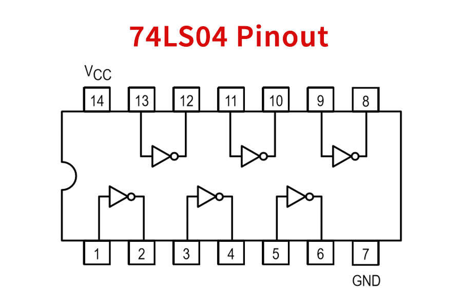
74LS04 has 14 pins. The input pins of the inverting gates are pin 1, 3, 5, 9. 11 and 13. The six pins are the inputs of gates 1-6, respectively. The output pins of the inverting gates are pins 2, 4, 6, 8, 10 and 12. These are the output pins of gates 1-6. Pin 7 and 14 are shared terminals, pin 7 being the ground pin and pin 14 is the Vcc pin. The ground pin should be connected to the ground and the Vcc pin to a positive voltage.
Have a look at the pinout diagram above.
74LS04 Equivalents and Replacement Details
The equivalents of 74LS04 are74LS14 and CD7404. Any of these transistors can be configured to come up with a NOT gate.